Price:
8222 EUR
Contact
Massachusetts Institute of Technology
Description
To earn a Verified Certificate for this course, you must agree to the terms and conditions of End-User License Agreements for integrated photonics industry software (EPDA) and a process design kit (PDK) library, as accessed via the AIM Photonics Virtual Design Center online cloud computing website.
In addition to the Verified Certificate for the course, the registration fee includes two hundred hours of user access to the Design Center, for verified learners to work online with the industry-standard software and library to create an integrated photonics circuit design project. Because of this special inclusion, financial aid or other discounts will not be available for this course.
A limited number of design projects completed by verified learners are eligible for free submission to an AIM Photonics Institute photonic circuit fabrication run. Fabricated circuits are subsequently characterized at an AIM PIC testing workshop organized at Rochester Institute of Technology.
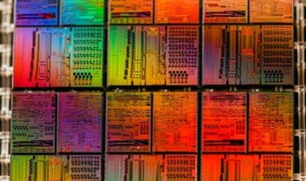
Photonics Integrated Circuits (PICs) are analogs to the computer microprocessor chip, poised to partner light-manipulating optical devices and transistor-based electronics for a vast array of modern applications in cloud computing, high-speed mobile wireless, smart sensing, augmented imaging, and quantum communications. PIC circuits create, guide, sort, and read information as signals of light, routed through a dizzying maze of hundreds of devices packed in an area about a millimeter on its side.
How can you design a circuit brimming with so much device density and interconnectedness, all by yourself? How can you do this design reliably, time and time again? How do you ensure your circuit is consistent with the design of others, so that you can both interpret each other’s chip architectures and applications?
Welcome to fabless photonics, the new paradigm for designing high-fidelity PICs.
This course introduces you to PIC design using a standardized Process Design Kit (PDK) library as your builders’ rulebook, and Electronic Photonic Design Automation (EPDA) software as your architecture tools. You’ll be guided through a step-by-step sequence giving you mastery to
model silicon photonic devices;
simulate a PIC;
layout the PIC chip; and
Design Rule Check (DRC) to revise layout into a final blueprint for PIC fabrication.
The course concludes with the creation of a verified “tape-out” design blueprint, ready for potential submission to a Multi-Project Wafer run at the AIM Photonics Institute—the world’s leading 300mm fabrication facility for high performance silicon PICs.
The course is structured around the design of a basic transceiver, and starts off with an overview of fabless PIC design followed by a review of passive photonic devices (waveguides, bends, splitters/combiners, interferometers). You’re then walked through the process of designing the transceiver chip with a focus on two active devices (electro-optic modulator, photodetector). The course highlights device compact models as the PDK methodology for flexible simulation and layout of PIC chip designs, and rigorously trains you in EPDA industry-standard software from Synopsys, Lumerical, Mentor Graphics, and the freeware KLayout.
The course runs for an initial three weeks of instruction (self-paced video lectures, homework, design project milestones, and a weekly synchronous webinar); followed by a two-week hiatus during which verified learners continue to have cloud access to the Design Center; and concludes with a final three weeks of instruction. Verified learners may elect to create a nominal PIC circuit design project in tandem with course instruction; or propose their own original circuit design (compatible with the AIM Education PDK component library), subject to instructor approval.
Completion of the course shows your professional engineer-level design aptitude in fabless integrated photonics, for leading edge industrial applications poised to transform modern manufacturing and the global economy in the next two decades.
Specific details
Category of Education
Technology and Engineering
